ADN8810
Rev. A | Page 14 of 16
5V
TO OTHER 5V
DIGITAL LOGIC
LOGIC GROUND
RETURN
3V
GND
POWER SUPPLY
ADN8810
AVDD
AVSS
LOAD
GND
IOUT
LOAD
DVDD
PVDD DVSS
DGND
Figure 23. Star Supply and Ground Technique
To improve thermal dissipation, the slug on the bottom of the
LFCSP package should be soldered to the PC board with
multiple vias into a low noise ground plane. Connecting these
vias to a copper area on the bottom side of the board will
further improve thermal dissipation.
Use identical trace lengths for the two output sense resistors.
These lengths are shown as X and Y in Figure 24. Differences in
trace lengths cause differences in parasitic series resistance.
Because the sense resistors can be as low as 1.37 ? small
parasitic differences can lower both the output current accuracy
and the output impedance. Application Note AN-619 shows a
good layout for these traces.
FB
IOUT
R
SN
R
SN
R
SN
TO LOAD
X
Y
ADN8810
SUGGESTED PAD LAYOUT FOR CP-24 PACKAGE
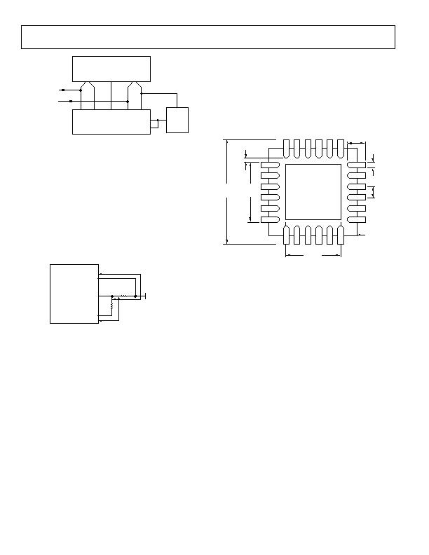
Figure 25 shows the dimensions for the PC board pad layout for
the ADN8810. The package is a 4 mm ?4 mm, 24-lead LFCSP.
The metallic slug underneath the package should be soldered to
a copper pad connected to AVSS, the lowest supply voltage to
the ADN8810. For single-supply applications, this is ground.
Use multiple vias to this pad to improve the thermal dissipation
of the package.
0.027
(0.69)
0.011
(0.28)
0.020
(0.50)
PACKAGE
OUTLINE
DIMENSIONS ARE SHOWN
IN INCHES AND (MM).
CONTROLLING DIMENSIONS ARE IN MILLIMETERS
0.004
(0.10)
0.827
(2.1) SQ
0.109
(2.78)
0.172
(4.36)
Figure 25. Suggested PC Board Layout for CP-24 Pad Landing
Figure 24. Use Identical Trace Lengths for Sense Resistors
发布紧急采购,3分钟左右您将得到回复。
相关PDF资料
ADP2140ACPZ3328R7
IC REG DL BCK/LINEAR 10LFCSP
ADP5022ACBZ-6-R7
IC REG TRPL BCK/LINEAR 16WLCSP
ADP5041ACPZ-1-R7
IC REG TRPL BCK/LINEAR 20-LFCSP
ADP5042ACPZ-2-R7
IC REG TRPL BCK/LINEAR 20LFCSP
ADT6402SRJZ-RL7
IC TEMP SENS TRIP PT PP SOT-23-6
ADT6501SRJZP085RL7
IC TEMP SENSOR MICROPWR SOT23-5
ADT7302ARTZ-500RL7
IC SENSOR TEMP 13BIT DGT SOT23-6
ADT7310TRZ
IC TEMP SENSOR 16BIT SPI 8SOIC
相关代理商/技术参数
ADN8810-EVAL
制造商:Analog Devices 功能描述:- Bulk
ADN8810XCP
制造商:Analog Devices 功能描述:- Bulk
ADN8820
制造商:Analog Devices 功能描述:LASER DRVR 1CH 48LFCSP - Trays
ADN8820ACP
制造商:Analog Devices 功能描述:LASER DRVR 1CH 48LFCSP - Bulk
ADN8820-REEL7
制造商:AD 制造商全称:Analog Devices 功能描述:EDFA and CW Laser Controller
ADN8830
制造商:AD 制造商全称:Analog Devices 功能描述:Thermoelectric Cooler Controller
ADN8830ACP
制造商:Analog Devices 功能描述:Temp Sensor Digital 32-Pin LFCSP EP 制造商:Rochester Electronics LLC 功能描述:HIGH PRECISION/EFFICIENCY TEC CONTROLLER - Bulk
ADN8830ACP-REEL
制造商:Analog Devices 功能描述:Temp Sensor Digital 32-Pin LFCSP EP T/R
